- 您现在的位置:买卖IC网 > Sheet目录526 > STD5406NT4G (ON Semiconductor)MOSFET N CH 40V 70A DPAK
�� �
�
�NTD5406N,� STD5406N�
�Power� MOSFET�
�40� V,� 70� A,� Single� N� ?� Channel,� DPAK�
�Features�
�?� Low� R� DS(on)�
�?� High� Current� Capability�
�?� Low� Gate� Charge�
�?� AEC� ?� Q101� Qualified� and� PPAP� Capable� ?� STD5406N�
�?� These� Devices� are� Pb� ?� Free� and� are� RoHS� Compliant�
�Applications�
�?� Electronic� Brake� Systems�
�?� Electronic� Power� Steering�
�?� Bridge� Circuits�
�V� (BR)DSS�
�40� V�
�http://onsemi.com�
�R� DS(ON)� TYP�
�8.7� m� Ω� @� 10� V�
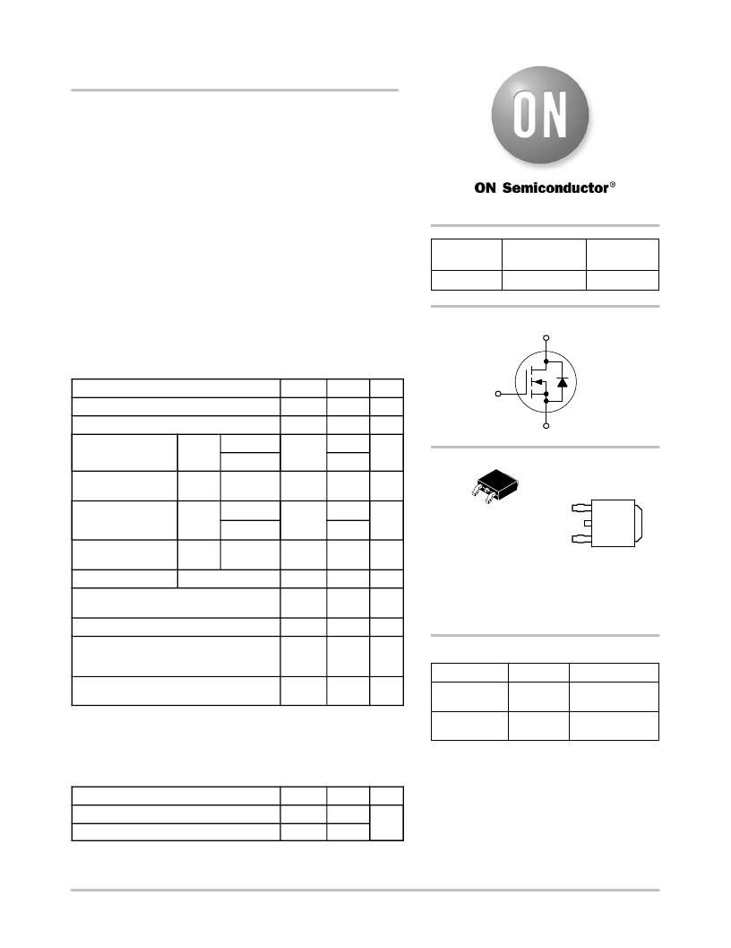
�N� ?� Channel�
�D�
�I� D� MAX�
�(Note� 1)�
�70� A�
�MAXIMUM� RATINGS� (T� J� =� 25� °� C� unless� otherwise� stated)�
�Parameter�
�Drain� ?� to� ?� Source� Voltage�
�Gate� ?� to� ?� Source� Voltage�
�Symbol�
�V� DSS�
�V� GS�
�Value�
�40�
�±� 20�
�Unit�
�V�
�V�
�G�
�S�
�Continuous� Drain�
�Current� ?� R� q� JC�
�Power� Dissipation� ?�
�R� q� JC�
�Continuous� Drain�
�Current� ?� R� q� JA�
�(Note� 1)�
�Power� Dissipation� ?�
�R� q� JA� (Note� 1)�
�Steady�
�State�
�Steady�
�State�
�Steady�
�State�
�Steady�
�State�
�T� C� =� 25� °� C�
�T� C� =� 125� °� C�
�T� C� =� 25� °� C�
�T� A� =� 25� °� C�
�T� A� =� 125� °� C�
�T� A� =� 25� °� C�
�I� D�
�P� D�
�I� D�
�P� D�
�70�
�40�
�100�
�12.2�
�7.0�
�3.0�
�A�
�W�
�A�
�W�
�4�
�1� 2�
�3�
�DPAK�
�CASE� 369C�
�STYLE� 2�
�1�
�MARKING�
�DIAGRAM�
�YWW�
�54�
�06NG�
�Pulsed� Drain� Current� t� p� =� 10� m� s�
�Operating� Junction� and� Storage� Temperature�
�Source� Current� (Body� Diode)� Pulsed�
�I� DM�
�T� J� ,�
�T� STG�
�I� S�
�150�
�?� 55� to�
�175�
�63.5�
�A�
�°� C�
�A�
�Y�
�WW�
�5406N�
�G�
�=� Year�
�=� Work� Week�
�=� Specific� Device� Code�
�=� Pb� ?� Free� Device�
�Single� Pulse� Drain� ?� to� Source� Avalanche�
�Energy� ?� (V� DD� =� 50� V,� V� GS� =� 10� V,� I� PK� =� 30� A,�
�L� =� 1� mH,� R� G� =� 25� W� )�
�EAS�
�450�
�mJ�
�ORDERING� INFORMATION�
�Device� Package� Shipping� ?�
�T� L�
�Lead� Temperature� for� Soldering� Purposes� 260� °� C�
�(1/8”� from� case� for� 10� s)�
�Stresses� exceeding� Maximum� Ratings� may� damage� the� device.� Maximum�
�Ratings� are� stress� ratings� only.� Functional� operation� above� the� Recommended�
�Operating� Conditions� is� not� implied.� Extended� exposure� to� stresses� above� the�
�Recommended� Operating� Conditions� may� affect� device� reliability.�
�THERMAL� RESISTANCE� RATINGS� (Note� 1)�
�NTD5406NT4G� DPAK� 2500� /� Tape� &� Reel�
�(Pb� ?� Free)�
�STD5406NT4G� DPAK� 2500� /� Tape� &� Reel�
�(Pb� ?� Free)�
�?For� information� on� tape� and� reel� specifications,�
�including� part� orientation� and� tape� sizes,� please�
�refer� to� our� Tape� and� Reel� Packaging� Specifications�
�Brochure,� BRD8011/D.�
�Parameter�
�Junction� ?� to� ?� Case� (Drain)�
�Junction� ?� to� ?� Ambient� (Note� 1)�
�Symbol�
�R� θ� JC�
�R� θ� JA�
�Max�
�1.5�
�49�
�Unit�
�°� C/W�
�1.� Surface� mounted� on� FR4� board� using� 1� sq� in� pad� size,�
�(Cu� Area� 1.127� sq� in� [2� oz]� including� traces).�
�?� Semiconductor� Components� Industries,� LLC,� 2013�
�August,� 2013� ?� Rev.� 6�
�1�
�Publication� Order� Number:�
�NTD5406N/D�
�发布紧急采购,3分钟左右您将得到回复。
相关PDF资料
SUD17N25-165-E3
MOSFET N-CH D-S 250V TO252
SUD19N20-90-T4-E3
MOSFET N-CH D-S 200V TO252
SUD19P06-60L-E3
MOSFET P-CH D-S 60V TO252
SUD23N06-31-T4-GE3
MOSFET N-CH D-S 60V TO252
SUD23N06-31L-E3
MOSFET N-CH D-S 60V TO252
SUD25N15-52-T4-E3
MOSFET N-CH D-S 150V TO252
SUD35N05-26L-E3
MOSFET N-CH D-S 55V TO252
SUD40N02-08-E3
MOSFET N-CH D-S 20V TO252
相关代理商/技术参数
STD5407NT4G
功能描述:MOSFET NFET 40V SPCL TR RoHS:否 制造商:STMicroelectronics 晶体管极性:N-Channel 汲极/源极击穿电压:650 V 闸/源击穿电压:25 V 漏极连续电流:130 A 电阻汲极/源极 RDS(导通):0.014 Ohms 配置:Single 最大工作温度: 安装风格:Through Hole 封装 / 箱体:Max247 封装:Tube
STD540BLK
功能描述:LED 安装硬件 .2" DIA. .54" BLACK RoHS:否 制造商:Bivar 产品:LED Mounting Clips LED 大小:5 mm 材料:Nylon 颜色:Black 主体长度:4.4 mm 面板厚度尺寸: 封装:Bulk
STD550BLK
功能描述:LED 安装硬件 .2" DIA X .55" BLACK RoHS:否 制造商:Bivar 产品:LED Mounting Clips LED 大小:5 mm 材料:Nylon 颜色:Black 主体长度:4.4 mm 面板厚度尺寸: 封装:Bulk
STD550BLK-PK10
制造商:Visual Communications Company (VCC) 功能描述:STANDOFF
STD550BLK-PK1000
制造商:Visual Communications Company (VCC) 功能描述:STANDOFF
STD55N4F5
功能描述:MOSFET N-Ch 40V 7.3 m" 40A STripFET V RoHS:否 制造商:STMicroelectronics 晶体管极性:N-Channel 汲极/源极击穿电压:650 V 闸/源击穿电压:25 V 漏极连续电流:130 A 电阻汲极/源极 RDS(导通):0.014 Ohms 配置:Single 最大工作温度: 安装风格:Through Hole 封装 / 箱体:Max247 封装:Tube
STD55NH2LL
制造商:未知厂家 制造商全称:未知厂家 功能描述:N-CHANNEL 24V - 0.008 OHM - 55A DPAK/IPAK ULTRA LOW GATE CHARGE STRIPFET POWER MOSFET
STD55NH2LL_06
制造商:STMICROELECTRONICS 制造商全称:STMicroelectronics 功能描述:N-channel 24V - 0.010ohm - 40A - DPAK/IPAK Ultra low gate charge STripFET TM Power MOSFET